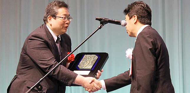
Tohoku University's Tetsuo Endoh, Tokyo Electron Limited's Gishi Chung and Keysight Technologies Inc.'s Masaki Yamamoto have been awarded Japan's Prime Minister's Award for Contribution to Industry-Academia-Government Collaboration.
The award recognizes outstanding achievements or pioneering efforts in industry-academia-government collaboration, especially by leaders in businesses, academia and public research institutions.
The collaboration brought expertise from scientists at Tohoku University and partnered them with major global companies Tokyo Electron and Keysight Technologies to research and develop innovative integrated electronics systems. Together, the group has developed high tech equipment for manufacturing and evaluating STT-MRAM (*1).
"We are delighted that our research with consortium members has been successful," says Professor Endoh, Director of the Center for Innovative Integrated Electronic Systems (CIES) at Tohoku University. "The CIES' global consortium is unique, with a system that makes it easier for academic, industry and government organizations to collaborate. These partnerships are essential for advancing the research and application of integrated spintronic devices worldwide."
For his part in the joint effort, Endoh has helped establish an R&D hub for advanced integrated circuits - CIES' global consortium - at Tohoku University. As a financially independent and self-sustainable operation, the CIES consortium provides a successful example for R&D management in universities.
The consortium allows two-part contracts with contributing companies: the first part consisting of basic rules for all members, while the second part takes into account individual requests, allowing flexibility within a united framework. Intellectual Property of core technologies is also managed at CIES so that they can provide free licenses for all participants. Currently the consortium has more than 30 members.
Endoh has pioneered 3D NAND memory (*2) research, and contributed to its mass production. The large capacity storage technology is widely used in USB drives, SD cards and SSDs.
World class manufacturers of semiconductor production equipment, Tokyo Electron Limited, led by Senior Vice President Gishi Chung, was acknowledged for its part in developing equipment for manufacturing STT-MRAM. Similarly, Keysight Technologies spearheaded by the vice president and general manager of Keysight's Hachioji Semiconductor Test Division, Masaki Yamamoto, has developed equipment to evaluate STT-RAM. Both companies have launched sales of the equipment, a move which forecasts STT-RAM as the future of high performance non-volatile memory. This will make manufacturing the technology possible on a global scale.
The Cabinet Office of the Japanese Government has played a central role in identifying and honoring successful cases of academic-industry-government collaboration since 2003.
(*1) STT-MRAM (Spin Transfer Torque - Magnetoresistive Random Access Memory): A memory device that uses magnetoresistance--a material's tendency to change its electrical resistance when a magnetic field is applied externally. The device is capable of high-speed random access, and consumes very little power as it retains the data even when the power is off. Because of these features, STT-MRAM is gaining traction as the next-generation technology for such applications as embedded memory, main memory and logic.
(*2) 3D NAND Memory: Semiconductor storage memory staked memory cells with vertical MOSFET. It's expected to be an important next-generation memory technology due to its high density - replacing existing planer-type NAND memory. Major semiconductor chip manufacturers in Japan and overseas have already begun sample shipments.
- About the Center for Innovative Integrated Electronic Systems at Tohoku University
The Center for Innovative Integrated Electronic Systems (CIES) was established as the first research base of the Science Park at Tohoku University's Aobayama campus in October 2012. The Center was created to research innovative integrated electronic systems with energy-saving technologies, drawing on the research knowledge base at Tohoku University and its vast experience in academic-industrial collaborations. CIES was the first research center at a Japanese university to have a 300mm wafer process line and characterization tools that are compatible with industrial R&D labs. CIES operates out of cutting-edge facilities as a base for innovations between Tohoku University and multinational corporations.
CIES has official government support, and is included in Sendai City's special zone for the promotion of private investments - a business model for supporting local enterprises.
Contact:
Yoichi OshimaCenter for Innovative Integrated Electronic Systems
Email: support-office@cies.tohoku.ac.jp

