
Researchers at Tohoku University have developed guidelines for a single-nanometer magnetic tunnel junction (MTJ), allowing for performance tailoring to meet the requirements of diverse applications, ranging from AI/IoT to automobiles and space technologies. The breakthrough will lead to high-performance spintronic non-volatile memory, compatible with state-of-the-art semiconductor technologies. The details were published in the journal npj Spintronics on January 4, 2024.
The key characteristic of non-volatile memory is its ability to retain data in the absence of an external power source. Consequently, extensive development efforts have been directed towards non-volatile memory because of its ability to reduce power consumption in semiconductor integrated circuits (ICs). Performance requirements for non-volatile memory vary according to specific applications. For instance, AI/IoT applications demand high-speed performance, while automotive and space technologies prioritize high retention capabilities.
Spin-transfer torque magnetoresistive random access memory (STT-MRAM), a type of non-volatile memory technology that stores data by utilizing the intrinsic angular momentum of electrons, known as spin, possesses the potential to address some of the limitations associated with existing memory technologies. The basic building block of STT-MRAM is the magnetic tunnel junction (MTJ): two ferromagnetic layers separated by a thin insulating barrier. Scientists have long tried to meet the challenge of making MTJs smaller whilst meeting performance requirements, but many problems remain.
STT-MRAM, employing MTJs with dimensions in the range of several tens of nanometers, has been successfully developed for automotive semiconductors using 1X nm technology nodes. Looking ahead to future nodes, however, there is a need to scale down MTJs to single-digit nanometers, or X nm, while ensuring the capability to tailor performance according to specific applications.
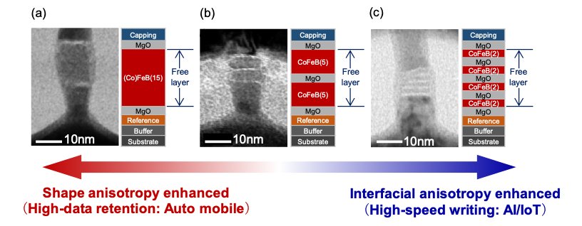
To do this, the research group designed a means to engineer single-nanometer MTJs with a CoFeB/MgO stack structure, a de facto standard material system. Varying the individual CoFeB layer thickness and the number of [CoFeB/MgO] stacks allowed them to control the shape and interfacial anisotropies independently - something crucial for achieving high-retention and high-speed capabilities, respectively.
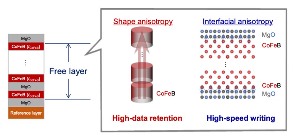
As a result, the MTJ performance can be tailored for applications ranging from retention-critical to speed-critical. At the size of single nanometers, shape-anisotropy enhanced MTJs demonstrated high retention (> 10 years) at 150°C, while interfacial-anisotropy enhanced MTJs achieved fast speed switching (10 ns or shorter) below 1 V.
"Since the proposed structure can be adapted to existing facilities in major semiconductor factories, we believe that our study provides a significant contribution to the future scaling of STT-MRAM," said Junta Igarashi, one of the lead authors of the study.
Principal Investigator Shunsuke Fukami added that "Semiconductor industries generally tend to be conscious of long-lasting scaling. In that sense, I think this work should send a strong message to them that they can rely on the future of STT-MRAM to help usher in a low-carbon society."
- Publication Details:
Title: Single-nanometer CoFeB/MgO magnetic tunnel junctions with high-retention and high-speed capabilities
Authors: Junta Igarashi, Butsurin Jinnai, Kyota Watanabe, Takanobu Shinoda, Takuya Funatsu, Hideo Sato, Shunsuke Fukami, and Hideo Ohno
Journal: npj Spintronics
DOI: 10.1038/s44306-023-00003-2
Contact:
Shunsuke Fukami
Research Institute of Electrical Communication
Email: s-fukami tohoku.ac.jp
Website: http://www.spin.riec.tohoku.ac.jp/en/