
A research team from Tohoku University and Kyocera Corporation has developed a new magneto-optical material - a nanocomposite magnetic garnet film - that can be deposited directly onto silicon substrates while delivering a magneto-optical figure of merit four times higher than conventional polycrystalline films. Using this material, the team demonstrated a monolithically integrated optical isolator on a silicon chip that matches the performance of conventional devices but with a far simpler, seed-layer-free structure. The breakthrough opens a practical path toward large-scale deployment of silicon photonics in AI-era data centers.
As artificial intelligence (AI) drives explosive growth in data center electricity consumption, silicon photonics - using light rather than electrical signals to transmit information - has emerged as a key next-generation technology. In particular, co-packaged optics (CPO), which integrates electronic and optical circuits within a single package, has emerged as a major focus of global development efforts for AI-era data center infrastructure.
Reliably operating these hybrid electronic-optical circuits requires on-chip optical isolators that block unwanted reflected light from returning to the laser source. The heart of such an isolator is a magnetic garnet thin film, which exploits the Faraday rotation effect - a phenomenon in which a magnetic field changes the orientation of light as it passes through certain materials. Integrating this magnetic garnet directly onto silicon has been one of the biggest obstacles in silicon photonics and CPO development for more than 30 years.
Single-crystalline garnet films deliver the highest magneto-optical performance, but they cannot be grown directly on silicon. They must be grown on a special garnet substrate first and then bonded to silicon - a complex process that does not fit well with mass production. Polycrystalline garnet films, in contrast, can be deposited directly on silicon but suffer high optical loss due to grain boundaries. This performance-versus-integration trade-off has been the integrated optical isolator field's central obstacle since the 1990s.
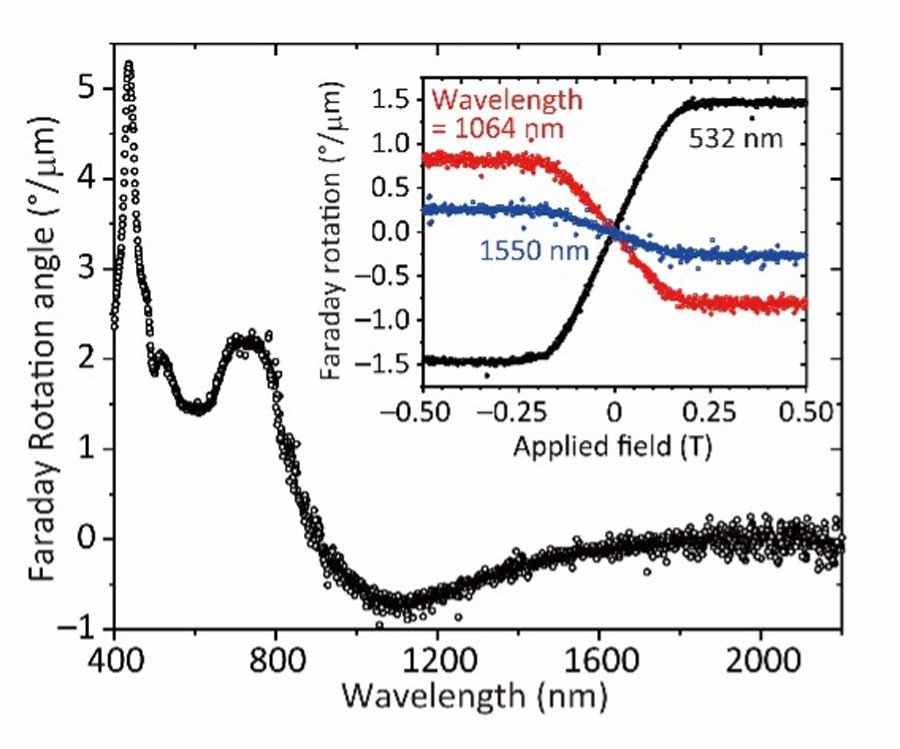
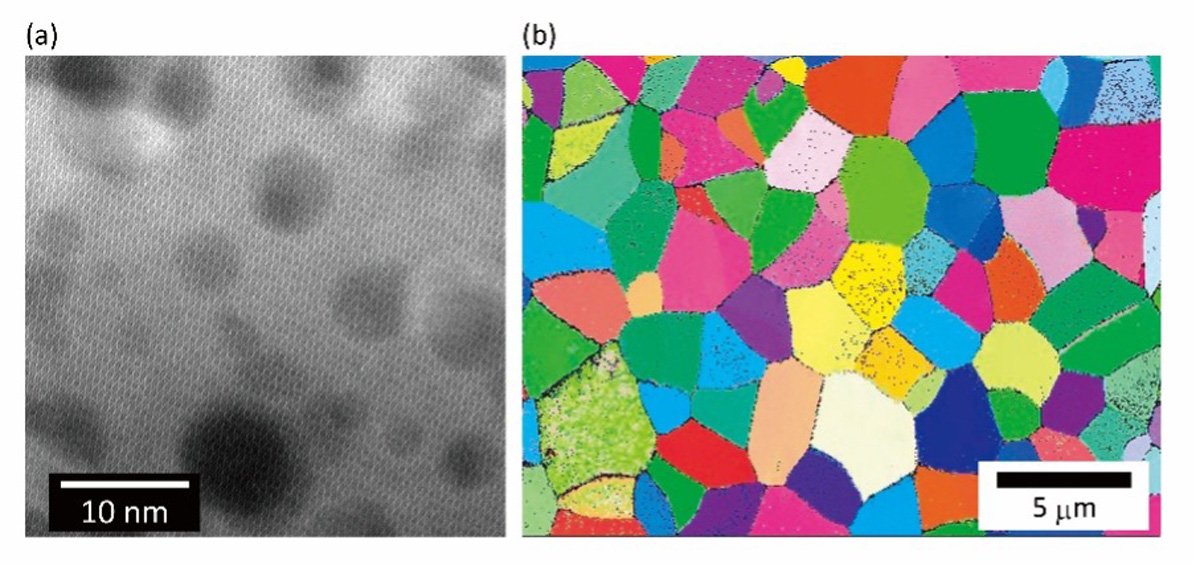
To overcome this bottleneck, the team extended the heating time during crystallization of an initially amorphous Ce:YIG film from 0.6 minutes (rapid heating from 25 to 800 °C) to 30 minutes - a process they call "gradual crystallization." This gradual heating produced a film with a previously unreported nanocomposite structure: cerium oxide (CeO₂) nanoparticles approximately 10 nm in diameter uniformly dispersed within a single-crystalline-like Ce:YIG matrix. The team attributes this structure to a "self-purification mechanism," in which excess cerium beyond what the Ce:YIG matrix can accommodate spontaneously precipitates as CeO₂ nanoparticles. This removes compositional non-stoichiometry and oxygen vacancies from the matrix, restoring crystal quality close to that of a single crystal. The resulting film achieves a magneto-optical figure of merit of 510°/dB at 1550 nm - approximately four times higher than the team's previously reported polycrystalline Ce:YIG films, and approaching the performance of much harder-to-integrate single-crystalline films.
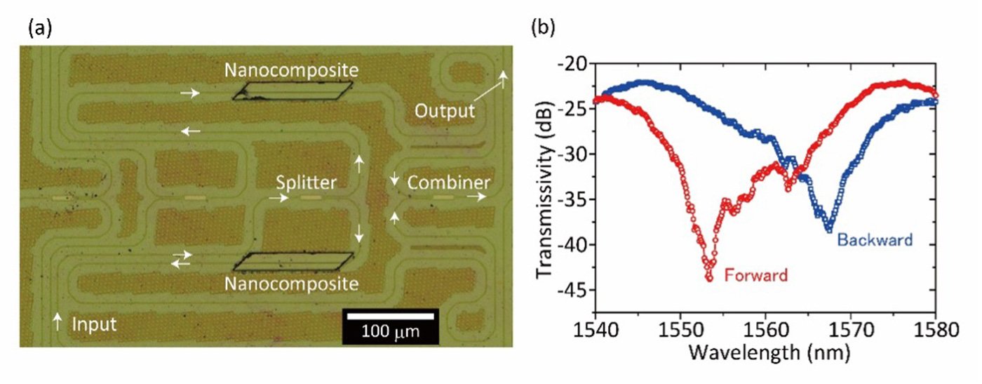
To demonstrate the practical value of this material, the team built an integrated optical isolator by depositing the nanocomposite film directly onto the silicon waveguide arms of an asymmetric Mach-Zehnder interferometer (AMZI) -- without any seed layer or wafer bonding step. The device delivered a magneto-optical insertion loss of 4.4 dB and an isolation ratio of 18.7 dB at 1555 nm, matching the performance of conventional integrated isolators that rely on seed layers or bonding processes, while using a far simpler single-film architecture.
"The 30-year gap between high-performance single-crystalline garnets and silicon-compatible polycrystalline garnets has been a long-standing barrier to practical on-chip optical isolators," said Associate Professor Taichi Goto from Tohoku University's Research Institute of Electrical Communication. "By tuning a single processing parameter - the crystallization heating rate - we found that excess cerium spontaneously self-organizes into nanoparticles that purify the surrounding garnet matrix. This simple yet powerful mechanism lets us approach single-crystalline-like performance using a process compatible with standard silicon photonics manufacturing. We believe this nanocomposite material will become a key building block for next-generation optical communication systems."
The findings were published in ACS Applied Optical Materials on June 12th and selected as an ACS Editors' Choice, a distinction awarded daily to one peer-reviewed article from across the ACS journal portfolio based on its broad scientific and public interest. Editors' Choice articles are made freely available to readers worldwide.
- Publication Details:
Title: Nanocomposite Garnet-Enabled Monolithically Integrated Magneto-Optical Isolator Using an Asymmetric Mach−Zehnder Interferometer
Authors: Tomoya Sugita, Hibiki Miyashita, Reona Motoji, Dan Maeda, Hiroki Yamamoto, Yuki Yoshihara, Kazushi Ishiyama, and Taichi Goto
Journal: ACS Applied Optical Materials (ACS Editors' Choice selection)
Contact:
Taichi Goto,
Research Institute of Electrical Communication, Tohoku University
Phone: +81-22-217-5489
Email: taichi.goto.a6 tohoku.ac.jp