
Professor Tetsuo Endoh, leading a group of researchers at Tohoku University, has announced the development of an MTJ (Magnetic Tunnel Junction) with 10 ns high-speed write operation, sufficient endurance (>1011), and with highly reliable data retention over 10 years at 1X nm size. Realizing a 1X nm STT-MRAM (Spin Transfer Torque-Magnetoresistive Random Access Memory) and NV(Non-Volatile)-Logic has wide application to a variety of fields.
Because STT-MRAM and NV-Logic with MTJ/CMOS hybrid technology offer low power consumption, they are essential constituents in semiconductor memory and logic such as processors. To put spintronics technology to practical use, higher speed write operation, lower power consumption, and greater endurance are required. Additional needs include data retention exceeding 10 years, a higher operation temperature, and excellent scalability. However, there has been a significant problem with data retention, which is often achieved at the expense of operational performance such as write speed, write power, endurance and so on. This problem has seriously limited the application field of STT-MRAM and NV-Logic.
For the application of 1X nm node STT-MRAM and NV-Logic to a wide variety of fields, the research team developed a new MTJ stack design technology and highly reliable fabrication technology for Quad interface type iPMA-MTJ (Quad-MTJ).
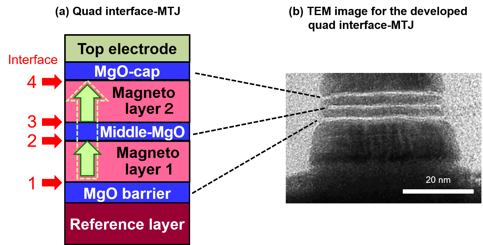
Figure 1: (a) Schematic and (b) TEM image of the developed quad -interface MTJ structure in this study. ⒸTohoku University
Using the new technologies - first proposed and demonstrated by the same team last year - resulted in a successful fabrication of advanced Quad-MTJ (Figs. 1a and 1b). The research team has now been able to demonstrate that the current write density of Quad-MTJ can be reduced by over 20% at a 10ns high speed write operation in comparison with the conventional Double-MTJ (Fig. 2a) - even though the thermal stability factor of Quad-MTJ is 2 times larger than Double-MTJ (Fig. 2b). In other words, the data retention of Quad-MTJ can be maintained for a period exceeding 10 years and at a higher operating temperature than Double-MTJ. Moreover, Quad-MTJ achieved satisfactory endurance levels (over 1011 Fig. 3), performing better than Double-MTJ, even though the data retention of Quad-MTJ is superior to that of Double-MTJ.
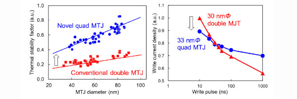
Figure 2: (a) Thermal stability factor of the novel quad-MTJ structure compared with those with the conventional double-MTJ structure. (b) Writing current density of 33nm-diameter quad MTJs compared with those with the 30nm-diameter double MTJs. ⒸIEEE & Tohoku University
The research team states that the advanced Quad-MTJ overcomes the serious issue of conventional Double-MTJ in several ways: the dilemma between data retention and many kinds of operation performance such as write speed, write power, endurance and so on.
As a result, these developed Quad-MTJ technologies, 1X nm STT-MRAM and NV-Logic with MTJ/CMOS hybrid technology will open a new spintronics base LSI suitable for wide applications including low-end fields (such as IoT systems and sensor network systems); high-end fields (such as AI systems and image processing systems); and the field of tolerance property for application in tougher environments (such as automobile parts, production facility systems and so on).
This research was supported by CIES's Industrial Affiliation with the STT MRAM program in the CIES Consortium of Tohoku University and CAO-SIP.
Results will be presented at this year's Symposia on VLSI Technology and Circuits as a virtual conference from June 14-19, 2020. In addition, the study was included in the "Technical Highlights from the 2020 Symposia on VLSI Technology & Circuits."
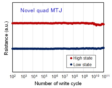
Figure 3: Endurance results of the 33 nm-diameter quad-MTJ. Although the quad-MTJ enhances the Δ by a factor of ~2, endurance of its MTJ exceeds at least 1011 ⒸIEEE & Tohoku University
- Publication Details:
Title: Scalability of Quad Interface p-MTJ for 1X nm STT-MRAM with 10 ns Low Power Operation, 10 years Retention and Endurance >1011
Authors: S. Miura, K. Nishioka, H. Naganuma, T. V. A. Nguyen, H. Honjo, S. Ikeda, T. Watanabe, H. Inoue, M. Niwa, T. Tanigawa, Y. Noguchi, T. Yoshizuka, M. Yasuhira, and T. Endoh
International Meeting: 2020 Symposia on VLSI Technology and Circuits
Contact:
Tetsuo Endoh (Profile)
Center for Innovative Integrated Electronic Systems, Tohoku University
Email: tetsuo.endoh cies.tohoku.ac.jp
Website: http://www.cies.tohoku.ac.jp/english/