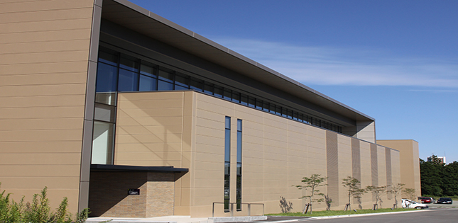
The Center for Innovative Integrated Electronics Systems (CIES) is a new international institute aimed at developing low-power technologies for a more energy-efficient society.
Located at the new Aobayama campus, CIES is the first Science Park of Tohoku University.
Researchers here develop innovative technologies, including the spin-transfer-torque-MRAM (STT-MRAM) and vertical MOSFET. These IC chips are expected to be in high global demand as they will be used in the next generation of consumer electronic devices such as personal computers, smart phones and tablets.
Natural Leader in Research and Development
Tohoku University has an outstanding record in the field of electronics. For research paper citations in 2013, the university was ranked sixth in the world for materials science and twelfth for physics. It also has the highest number of patent submissions among all universities in Japan.
Building on the university's strengths in spintronics, CIES has developed a number of technologies, as well as the knowledge required, to bring a product to prototype stage. It has also made efforts to fabricate test samples that are compatible with industrial R&D.
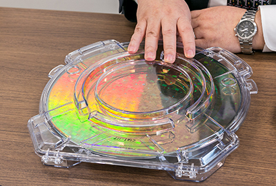
300mm wafer produced by CIES
"CIES has a high standard of productivity and Tohoku University has a good tradition in electronics studies," says Director of CIES Tetsuo Endoh. "That combination makes this an ideal place for both science and technology to develop together."
World's 2nd Academic Clean Room for 300mm Wafers
CIES is proudly operating a process line to produce 300mm wafers in its own clean room. The clean room is operated by Tohoku University and funded by a private grant from the semiconductor industry. It is only the second such academic facility in the world (the other being in the U.S.)
This facility allows researchers to study device characterization, including statistical and physical analyses, while facilitating smooth collaborations with industry players.
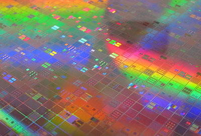
Integrated circuits in 300mm wafer produced by CIES team
One such collaboration - the development of the STT-MRAM prototype - is now a major international academic and industrial consortium, with CIES contributing its 300mm shuttle process.
The speed of progress at CIES has been impressive with its first lot of 300mm wafers created in November 2013, just seven months after the start of its clean room in April.
Innovation through Collaboration
As of March 2015, CIES has been working with more than 40 collaborators from all over the world.
Projects include JST ACCEL, a 2.5 billion yen JST-funded project led by CIES' Director Endoh. This ACCEL project aims to develop high performance DRAM and STT-MRAM with vertical BC-MOSFETs.
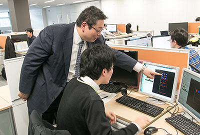
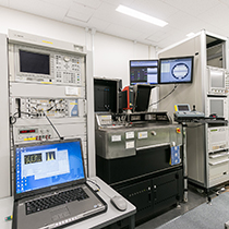
Supportive research environment at CIES
CIES makes collaboration easy by offering wide-ranging arrangements for its partners. For example, an information security system for balancing information accessibility and information firewall.
A free business license is also provided so that collaborators can take advantage of background intellectual properties (IPs). CIES manages the background IPs and bears the patent maintenance fees.
To make communication clearer and easier, all contracts are written in English.
Strong local government support
The local governments of Miyagi Prefecture and Sendai City support people who start up businesses in Sendai. Benefits include rent-free office space for the initial two years.
CIES has official government support, and is included in the city's special zones for the promotion of private investments.
The Center for Innovative Integrated Electronics Systems established in 2012 on the new Aobayama campus at Tohoku University.